RegFGC3 Type 10
Converter control crate
Control Crate
RegFGC3 is the name of the control crate for switch mode converters. The two parts of the word “Reg-FGC3” are derived from its main functions which are the power converter REGulation and the Function Generation Controller (version 3). The control crate consists of a backplane PCB that routes all signals from burndy connectors (power supply, inputs/outputs to the crate) to the different cards that can be plugged to it. You may read more information in the MPC project management EDMS folder and in the technical documentation EDMS folder.
- General-information
- Project mandate by Gilles Le Godec and Ben Todd
- Detailed Documentation
- Crate and Board Schematics
- Commissioning and Operation
Fault Chains
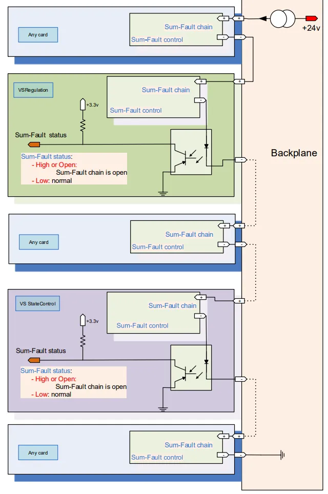
The RegFGC3 Crate implements 5 different fault chains. The chains comprise a current source generating 10mA. The current circulates through each one of the RegFGC3 removable cards (if a card is missing from a crate a termination board should provide a path for the chain current). Each removable card hosts a relays that can be used to open the respective chain. Each card also hosts an optocouplers for obtaining the status of the respective chain. The document EDMS 1526937 describes this architecture.
Inputs Outputs and Powering
The RegFGC3 interfaces with the external world through Burndy connectors
Main Circuit Breaker
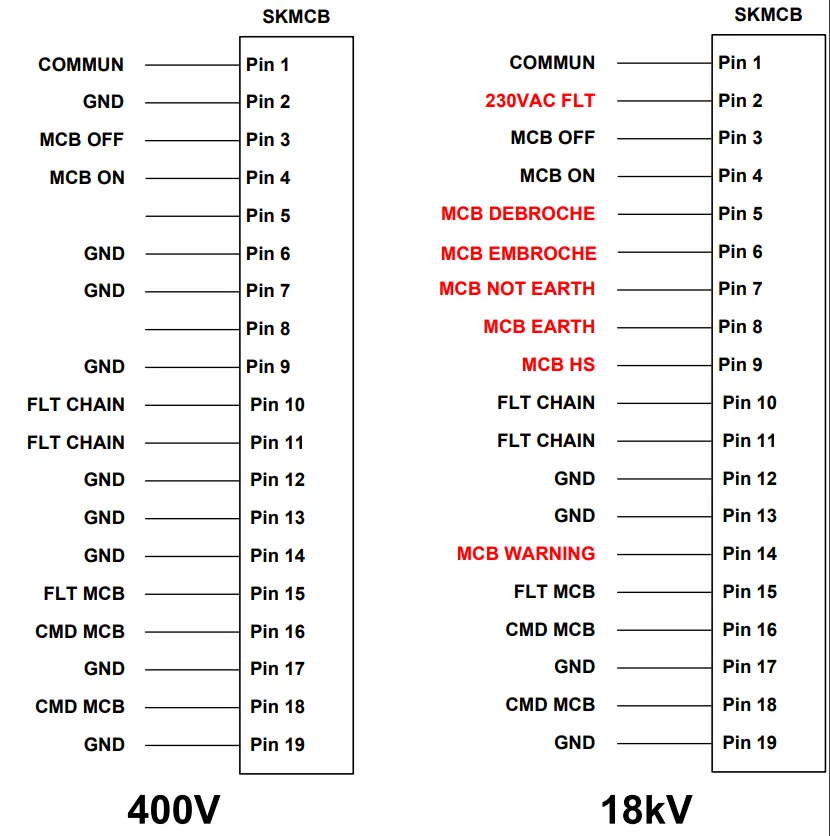
Interfacing with main circuit breakers of either 400V or18kV has been anticipated and is described by EDMS 1416518
Control Crate Cards
| DCCT PSU | DCCT V2V or I2V | Extension | FGC3 | VS State Control | VS Regulation | VS Meas. 1 | VS Meas. 2 | VS An. intlk 1 | VS An. intlk 1 | empty | VS dig. intlk 1 | VS dig. intlk 2 | Termin. | RegFGC3 PSU | Termin. |
|---|---|---|---|---|---|---|---|---|---|---|---|---|---|---|---|
| EDA | |||||||||||||||
| .sch | V2V I2V | .sch manual | sch manual |
Diagnostic cards
| Picture | 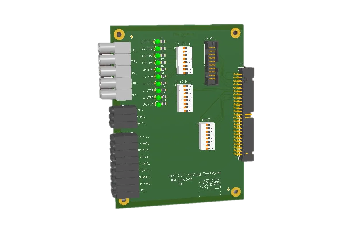 | |||
| Design reference | EDA-02296-V1-0 | EDA- | EDA | |
| Used with | VS state machine, VS regulation DSP, VS digital interlock | VS Measurement | VS Analog Interlock | |
| Guide | EDMS 1416522 |
VS State Machine card
The complete card (EDA-2261-v4-1) pin-out (inputs-outputs) with description can be found in EDMS 1731664. The following table indicates the card signals that can be accessed using the diagnostic (front-panel board).
| Front Panel Test Card Dip switch (d1,d2,d3,d4) | Front Panel Test Card Dip switch (d1,d2,d3,d4) | |||
|---|---|---|---|---|
| 1 | VS_RUN_NOT 0: converter on | FAULT_SUM_MEM_HW 1: any fault detected by any card | ||
| 2 | VS_RESET_NOT 1->0->1 while reseting | FAULT_INTERNAL 1:fault detected by internal FPGA | ||
| 3 | OUTPUT_BLOCK 1: pwd output disabled | FALT_FAST-PA 1: fault fast-PA detected by the card | ||
| 4 | VS_FAULT 1: fault on any of the crate cards | WARNINGS 1: warnings detected by the system | ||
| 5 | FASTPA_MEM 1: fault fastPA detected | FAULT_SUM_CHAIN_STATUS 1: status read of sum-fault chain | ||
| 6 | VS_EXTINTLK 1: fault from external source | FAST_BLOCKING_CHAIN_STATUS 1:status read of blocking-chain | ||
| 7 | POWER_ON 1: any voltage >50V | |||
| 8 | OP_BLOCKED 1: converter in blocking | FAULT_SUM_CMD 1: fault-sum chain opened by FPGA | ||
| 9 | VS_READY 1: converter ready for on (no fault) | FAST_BLOCKING_CMD 1: fault-blocking chain opened by FPGA | ||
| 10 | CARD_RESET_FAULTS rising edge during reset | OPEN_REQ_CMD 1: open-request chain opened by FPGA |
* to obtain cleaner signals on diagnostic card outputs disable LEDs using the respective DIP switches
Regulation DSP card
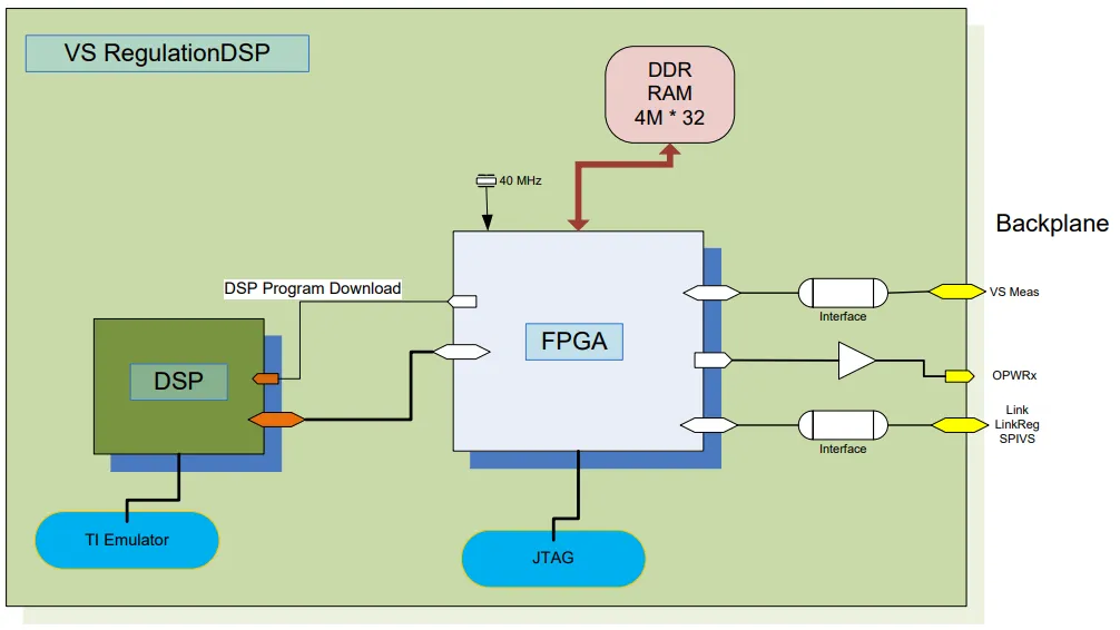
The DSP Regulation card is handling the regulation of the Voltage source. It receives a current reference from the FGC Controller Card and regulates the Power converter voltage to accomplish the required performance. It then generates the PWM controlling the semiconductor switches of the power part using an internal 30Mhz clock. The PWM signals are enabled or disabled by means of the FPGA on the card. An overview of the Card architectuire can be seen in the picture (EDMS 1541075)
The complete card (EDA-02262-V4-0) pin-out (inputs/outputs) with description can be found on EDMS 1731667. The following table indicates the card signals that can be accessed using the diagnostic (front-panel board).
| 1 | VS_RUN_NOT | FAULT_+15VOPWR | OPWR 01 | OPWR 11 not used | OPWR 21 |
| 2 | VS_RESET_NOT | control_reset_opwr | OPWR 02 | OPWR 12 boost | OPWR 22 |
| 3 | Control of OPWR +15v | OPWR 03 | OPWR 13 | OPWR 23 | |
| 4 | OPWR Not Enabled by FPGA | OPWR 04 | OPWR 14 | OPWR 24 | |
| 5 | FAULT_SUM_CHAIN_STATUS | OPWR 05 not used | OPWR 15 | ||
| 6 | FAST_BLOCKING_CHAIN_STATUS | OPWR 06 boost | OPWR 16 | ||
| 7 | OPWR Enabled by DSP | OPWR 07 | OPWR 17 not used | ||
| 8 | FAULT_SUM_CMD | OPWR 08 | OPWR 18 boost | ||
| 9 | FAST_BLOCKING_CMD | OPWR 09 | OPWR 19 | ||
| 10 | CARD_RESET_FAULTS | OPEN_REQ_CMD | OPWR 10 | OPWR 20 | PWM SYNC |
* to obtain cleaner signals on diagnostic card outputs disable LEDs using the respective DIP switches
** the signals described on this table depend on the Regulation card FPGA programme version. They are valid for the IGBT converters